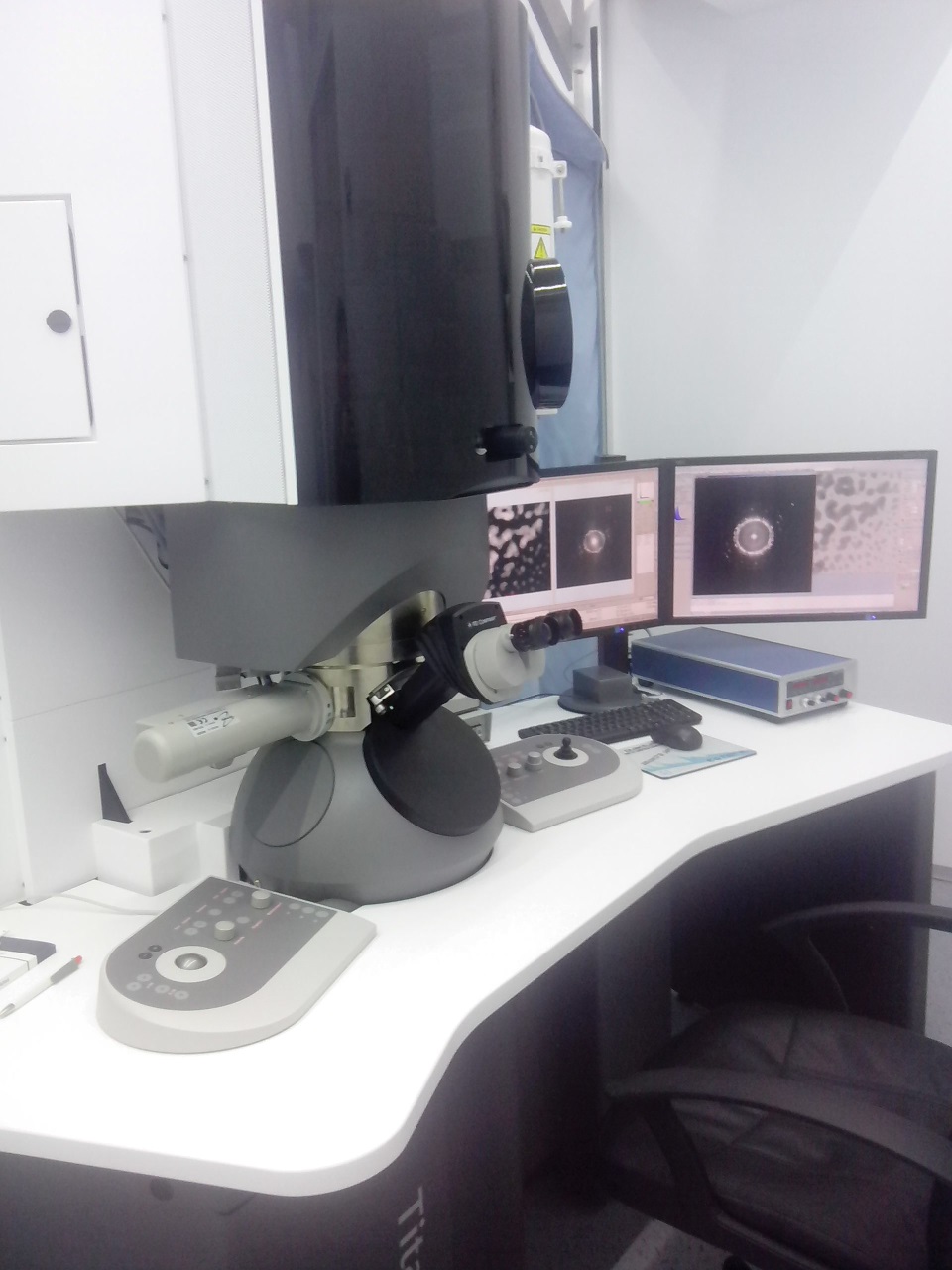
FEI Themis ETEM - FEG Scanning Transmission Electron Microscope
| Location: | Institute headquarters, Bratislava |
Main features
- operates in TEM and STEM mode
- atomic resolution combined with high analytical capabilities
- multi-signal detection from up to four signal simultaneously to accelerate scanning transmission electron microscopy (S/TEM) imaging
- Cs Probe Correctorfor sub-A resolution in STEM mode
- super X: High-sensitivity, windowless EDX detector system based on SDD technology
- electron energy loss spectroscopy (EELS)
- field-free imaging in Lorentz mode with 2nm resolution for magnetic property studies
- micro-tomography
- cryo-electron microscopy
Basic technical parameters
- accelerating voltage (X-FEG) – (80, 200, 300) kV
- resolution: 200 kV performance - TEM information limit ≤ 0.8 Å; HR-STEM resolution ≤ 0.8;
- EDX: output count rate up to 200 Kcps120 mm2 combined detector area, detection of all elements down to boron
- holders: single tilt holder
- double tilt holder
- cryo holder
- detectors: TEM - CMOS based FEI CETA camera; STEM- HAADF, BF, DF2, DF4; EDX – Super X windowless EDX; EELS – Enfiniumspektrometer